


Newsletter Subscribe
Enter your email address below and subscribe to our newsletter
Enter your email address below and subscribe to our newsletter
All voices matter
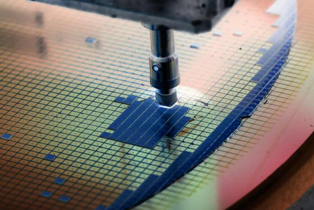
ASML, TSMC, and Belgian research hub Imec have jointly demonstrated a manufacturing-compatible integration flow for transistors built with two-dimensional materials on industry-standard 300mm wafers, achieving contact pitches as small as 50 nanometers. The results, presented at the 2026 Symposium on VLSI Technology and Circuits in Honolulu, Hawaii, mark the first time EUV lithography has been used to pattern 2D-material transistors at such aggressive dimensions in a full 300mm fab environment.techpowerup
The collaboration produced both n-type and p-type transistors using transition metal dichalcogenide channels — molybdenum disulfide for NMOS and tungsten diselenide for PMOS — fabricated side by side on the same wafer. The devices achieved active widths down to 75 nanometers and an equivalent oxide thickness of approximately 2 nanometers. Quasi-CMOS integration was accomplished through a die or small wafer transfer method that placed both channel materials on a single substrate.imec-int
Two-dimensional materials have long been studied as potential successors to silicon channels in advanced transistors because their atomically thin layers could enable better electrostatic control at the sub-nanometer scale. However, translating lab-scale results to production-sized wafers using standard equipment has remained a central challenge.eenewseurope
The demonstration builds on work presented at IEDM in December 2025, where Imec reported record-performing WSe₂-based p-type transistors developed in collaboration with TSMC, alongside 300mm-compatible process modules co-developed with Intel. That earlier effort showed maximum drive currents as high as 690 microamps per micrometer using a fab-compatible process flow.belganewsagency
According to Imec’s press release, the latest work brings “industry-ready 2D-material transistors closer” by combining EUV patterning capability from ASML with TSMC’s manufacturing expertise and Imec’s 300mm pilot line infrastructure.imec-int
The announcement arrives amid intensifying efforts across the semiconductor industry to prepare post-silicon technologies for eventual production. At the same VLSI symposium, Samsung presented its most aggressively scaled CFET architecture, Intel disclosed performance improvements to its 18A technology, and TSMC unveiled its A16 platform with backside power delivery slated for mass production in the fourth quarter of 2026. The 2D-material work, while earlier on the development timeline, signals that the ecosystem of lithography tools, materials, and integration techniques needed for a future manufacturing transition is beginning to take shape.vlsisymposium