


Newsletter Subscribe
Enter your email address below and subscribe to our newsletter
Enter your email address below and subscribe to our newsletter
All voices matter
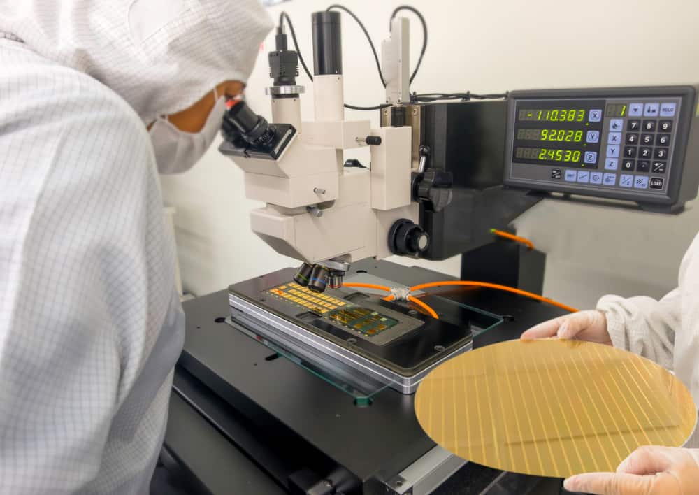
SemiAnalysis released the first public teardown from its new STEEL Lab (Teardown Engineering & Evaluation Lab) over the weekend, delivering a granular technical analysis of Huawei’s Kirin 9030 Pro built on SMIC’s most advanced N+3 process node. The report’s headline finding: SMIC N+3 achieves a minimum metal pitch of 32.5 nanometers on its M0 layer — roughly 10% tighter than the 36nm pitch on Intel’s shipping Panther Lake processors built on its 18A node. But SemiAnalysis itself called the comparison a “cherry picked metric,” cautioning that a single local routing layer does not determine which process is more advanced.kucoin
Through transmission electron microscopy, the STEEL Lab measured SMIC N+3’s Bohr logic density at 113.4 million transistors per square millimeter, slightly above TSMC’s N6 at 107.7 MTr/mm². Cell height shrank from 252nm on the prior N+2 node to 228nm, and contacted gate pitch fell from 63nm to 57nm. The density was achieved entirely through DUV lithography, without access to ASML’s EUV equipment, using self-aligned quadruple patterning on the M0 layer — a technique that requires far more masks, tighter overlay control, and greater cost than the double patterning TSMC uses for N6.odaily
While the density figures represent genuine progress, the Kirin 9030 remains well behind current leading mobile chips in performance and power efficiency. SemiAnalysis found the chip’s prime core IPC roughly matches Arm’s Cortex-X2 from 2021, while Apple’s latest M5 core holds a 2.7x absolute performance advantage. GPU performance from the Maleoon 935 reaches the level of 2022 Android flagships, slightly exceeding the Snapdragon 8+ Gen 1, but trails Qualcomm’s current Snapdragon 8 Elite Gen 5 by a factor of 2.4 to 2.6 times. The root cause, the report concludes, is not chip design but manufacturing process — Apple and Qualcomm benefit from TSMC’s N4 and N3P nodes, which offer fundamental advantages in power-frequency scaling.odaily
With conventional planar scaling increasingly constrained under U.S. export controls, Huawei has staked its roadmap on a different approach. At the IEEE ISCAS conference in Shanghai on May 25, Huawei semiconductor chief He Tingbo unveiled the Tau scaling law and the LogicFolding architecture, which aims to stack active logic layers vertically using fine-pitch hybrid bonding rather than relying on smaller transistors. Huawei’s roadmap targets a large-core frequency of 5GHz and an equivalent density of 295 MTr/mm² by 2031 — comparable to TSMC’s planned 14A-class node — with the first LogicFolding-enabled Kirin chips expected in fall 2026.actuia
SemiAnalysis expressed caution about this trajectory, noting that Huawei’s density calculations for stacked designs are based on package footprint rather than per-die metrics, making direct comparisons with conventional foundry nodes difficult. As the teardown concludes, export controls have not stopped China’s chip progress — but they have changed both the path and the cost of advancement.odaily