


Newsletter Subscribe
Enter your email address below and subscribe to our newsletter
Enter your email address below and subscribe to our newsletter
All voices matter
Samsung Electronics announced on Tuesday that its Semiconductor Research Center has demonstrated the world’s first 3D Stacked Field-Effect Transistor at a gate pitch of 42 nanometers, a breakthrough presented at the VLSI Symposium 2026 in Honolulu that earned the conference’s Best Paper award.sedaily
The paper, titled “First Demonstration of 3D Stacked FETs at Gate Pitch of 42nm Featuring Triple Stacked Nanosheet Channels for Advanced Logic Applications,” was selected as the top paper from more than 1,000 submissions to the symposium, one of the world’s three premier semiconductor conferences. The research was led by Samsung’s Logic TD Team under lead author Donghoon Hwang.linkedin
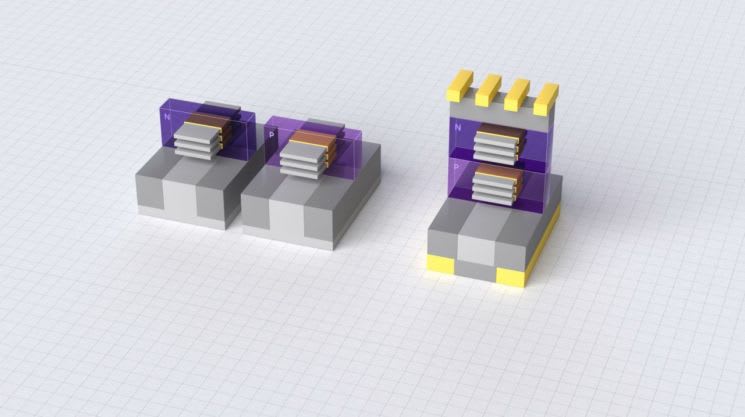
Traditional logic chips improve density by shrinking the horizontal spacing between transistors, but as dimensions approach physical limits, thin insulating layers begin to leak current. Samsung’s approach stacks N-type and P-type transistors vertically, theoretically doubling the number of transistors that can fit in the same area. The company employed triple-stacked nanosheet channels for both device types on a single wafer — the largest number of nanosheets ever demonstrated in a complementary FET structure.sedaily
The 42-nanometer gate pitch surpasses the previous industry minimum of 48 nanometers. Samsung said it solved the critical challenge of electrically isolating the upper and lower transistors through an intermediate dielectric layer and applied a direct connection between the stacked devices. The company noted that the concept of vertical stacking has already been proven in memory semiconductors through V-NAND flash and high-bandwidth memory, but this marks its first application to logic chips.news1
Samsung expects the technology to serve next-generation logic semiconductors for artificial intelligence and high-performance computing, where fitting more transistors per unit area can improve both processing power and energy efficiency. The company said it plans to continue research toward commercialization, though it did not specify a timeline for volume production.mk
The VLSI Symposium 2026 ran from June 14 to 18 in Honolulu, with presentations from Samsung, Intel, and TSMC all advancing competing approaches to 3D transistor stacking.ieee