


Newsletter Subscribe
Enter your email address below and subscribe to our newsletter
Enter your email address below and subscribe to our newsletter
All voices matter
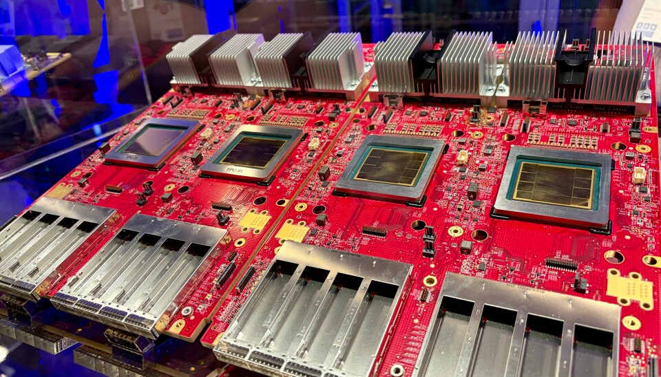
Samsung Electronics has secured chip manufacturing contracts from both Google and Neuralink, capitalizing on capacity constraints at rival TSMC to inject new momentum into its long-struggling foundry business.
Google is in talks with Samsung to manufacture a memory input-output die for its 10th-generation tensor processing unit, codenamed “Icefish,” according to a report by The Information first published on June 11. The chip would use Samsung’s 2-nanometer process technology, with TSMC handling the primary computing engine on its 1.4nm node. Mass production could begin as early as 2028, though the design remains in its early stages.koreaherald
Reuters reported that Google is also collaborating with MediaTek on the chip’s design. The arrangement reflects a broader industry trend of splitting chip production across multiple foundries as TSMC’s advanced-node capacity falls short of demand. TSMC Chairman C.C. Wei acknowledged in late 2025 that the company’s capacity was “about three times short” of what customers needed.reuters
Samsung has also begun developing Neuralink’s fourth-generation brain-computer interface chip, its first contract from the Elon Musk-backed neurotechnology company, according to South Korea’s Hankyung newspaper. The project, internally codenamed “O1,” uses Samsung’s 4-nanometer FinFET process and began research and development late last year.sammobile
Production of the first test chips started in May, with shipments scheduled for the first half of 2027 and mass production potentially beginning by year-end 2027. The fourth-generation chip is designed to enable two-way communication between the brain and electronic devices — a departure from earlier Neuralink chips that only interpreted brain signals to relay commands.wccftech
The wins come as Samsung positions itself as the only chipmaker capable of offering memory, logic manufacturing, and advanced packaging under one roof. The company began shipping industry-first 12-layer HBM4E memory samples to major customers in late May, delivering bandwidth of up to 3.6 terabytes per second.samsung
Samsung’s foundry utilization rates exceeded 80 percent in the first quarter of 2026, a one-year high, buoyed by contracts including a Tesla autonomous driving chip deal secured last year. Analysts expect the foundry division could return to profitability as early as 2027.kedglobal