


Newsletter Subscribe
Enter your email address below and subscribe to our newsletter
Enter your email address below and subscribe to our newsletter
All voices matter
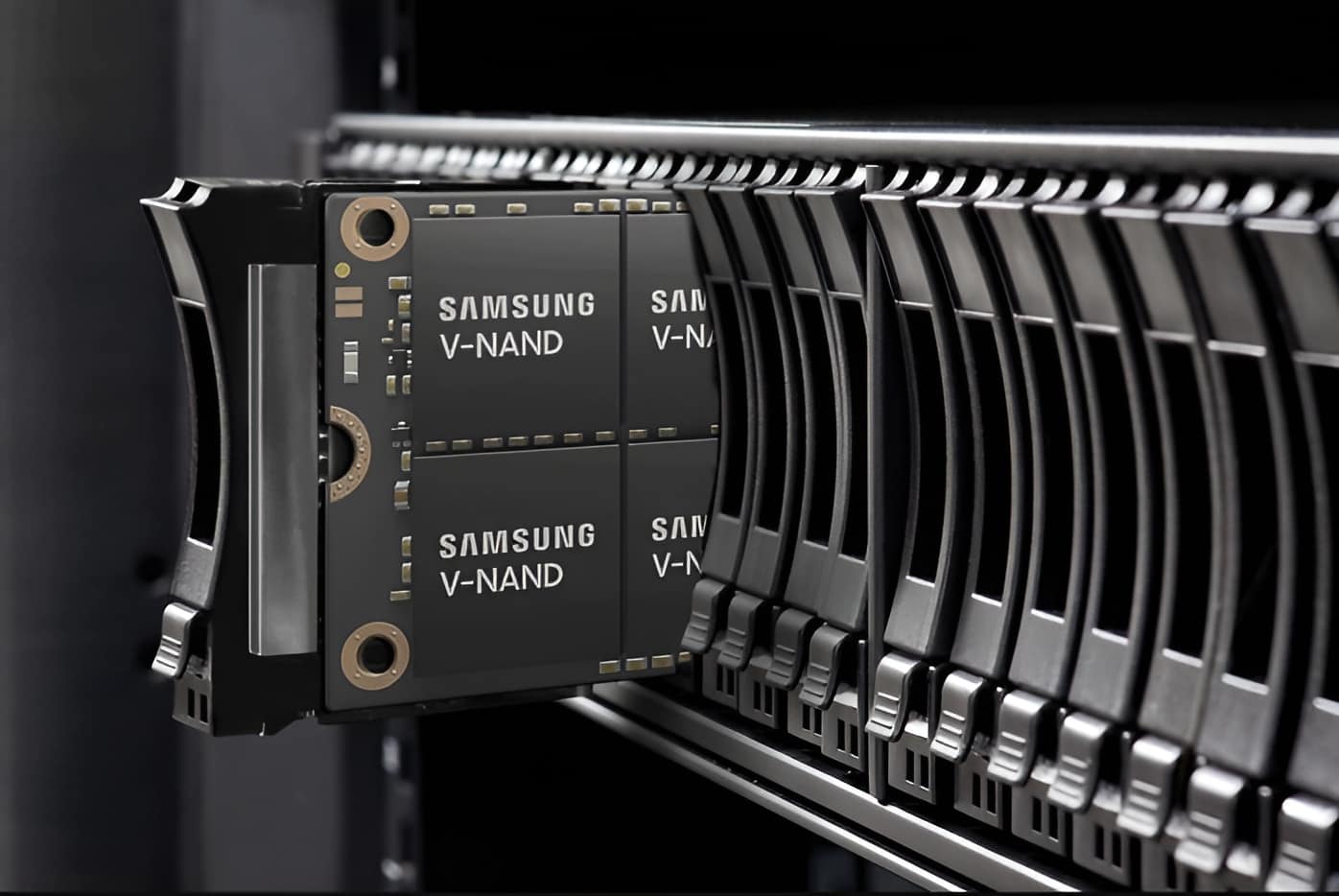
Samsung Electronics has developed the world’s first 900-layer V-NAND flash memory chip prototype, a milestone that brings the semiconductor industry closer to the 1,000-layer era and positions the South Korean firm to reassert its dominance in NAND flash storage.
According to a report from ETNews, Samsung created the 900-layer-class prototype using a technology called Cell Multi-Bonding (CMB), which fuses two 450-layer cell wafers into a single chip. The technique allows Samsung to dramatically increase storage density while reducing power consumption — qualities increasingly valued for AI computing workloads.sammobile
Samsung was the first company to commercialize 3D V-NAND flash chips in 2013, using a process that drilled and stacked microscopic holes in a single step. As stacking heights grew, the company encountered challenges including wafer warping and stack misalignment, which it addressed using an advanced Upper Chuck design and Overlay Correction technology. Samsung also improved its Bitline and Wordline structures to reduce power consumption and chip size.sammobile
The breakthrough comes as Samsung faces intensifying competition on two fronts. SK Hynix currently leads in the high-layer NAND segment with its 321-layer chips already in mass production. Meanwhile, China’s Yangtze Memory Technologies Co. (YMTC) has begun mass production of 294-layer NAND chips, supported by government investment and increasing localization of manufacturing equipment.jetstor
Samsung is simultaneously preparing for mass production of 400-layer tenth-generation NAND flash chips while pushing the 900-layer milestone in its research phase. Company executives have previously set a goal of exceeding 1,000 layers by 2030.sammobile
The drive toward higher layer counts reflects surging demand for storage driven by artificial intelligence workloads. High-density NAND is essential for the large-scale data storage and retrieval that AI systems require, making the layer-count race a proxy for competitiveness in the broader AI infrastructure market. Samsung’s prototype, while not yet ready for commercial production, signals that the company intends to lead the next generation of flash memory technology rather than cede ground to its rivals.sammyfans