


Newsletter Subscribe
Enter your email address below and subscribe to our newsletter
Enter your email address below and subscribe to our newsletter
All voices matter
A team at the University of Illinois Urbana-Champaign has demonstrated a method for building high-performance silicon circuits vertically, layer by layer, in a breakthrough that could offer the semiconductor industry a path forward as traditional transistor shrinking reaches its physical limits.
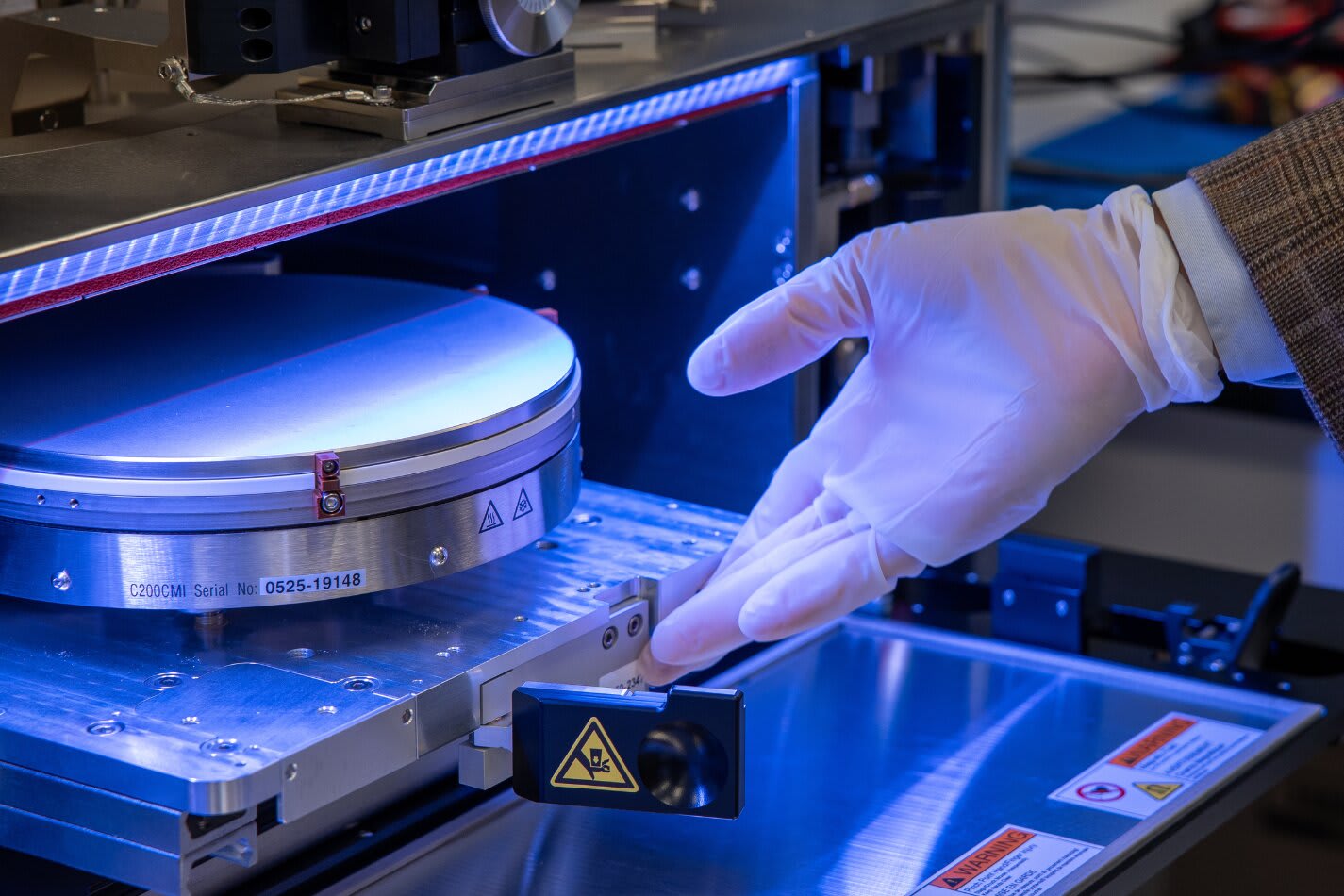
The research, published in Nature and led by materials science professor Qing Cao, introduces a process for monolithic three-dimensional integration using standard single-crystalline silicon — the same material already used across the chip industry. The technique relies on ultrathin silicon nanomembranes transferred onto completed circuit layers using a roll laminator at temperatures no higher than 200 degrees Celsius, well within the 400-degree thermal budget required to avoid damaging existing metal wiring beneath.analyticsinsight
Using this approach, the team fabricated three vertically stacked device layers, each containing 625 transistors, achieving yields of 98 to 100 percent even in an academic cleanroom. The transistors matched the performance of conventional silicon devices and outperformed alternative low-temperature materials by three to four times.illinois
Unlike existing chiplet-based approaches that bond separately fabricated wafers, monolithic 3D integration builds each layer directly atop the previous one, enabling 10 to 100 times denser vertical connections, smaller separations between layers, and nanometer-scale alignment accuracy. The researchers demonstrated working 3D logic circuits and static random-access memory cells that reduced circuit footprints by up to three times compared with equivalent flat designs.illinois
“It’s like replacing a sprawling suburb with high-rises: you get the same functionality, but the spatial footprint is reduced while making communication between layers faster and more efficient,” Cao said.illinois
The researchers are now working to transfer the technology to industrial semiconductor foundries, supported by partnerships with IBM, Intel, and TSMC through the university’s Center for Advanced Semiconductor Chips with Accelerated Performance.scienmag
“You can keep stacking layers beyond the three we demonstrated,” Cao said. “We now have a strong foundation for transferring this technology and demonstrating its immediate promise in an industrial semiconductor foundry.”illinois